Smith Chart from the Nutshell (Deep Theory + Practical Matching)
The Smith chart is not “just a chart” — it is a compact graphical calculator that hides heavy transmission-line algebra inside geometry. Once you learn what each curve means, you can solve impedance matching, input impedance, VSWR, and stub design problems in minutes with high confidence. This long-form tutorial is designed to feel like a mini-chapter: strong intuition, full derivations, and worked examples.
1) Why the Smith Chart exists
In DC/low-frequency circuits, wires are “electrically short” and you can treat interconnects as ideal. But as frequency rises, the physical length becomes comparable to wavelength, and the interconnect behaves like a transmission line. In that regime, voltage and current are waves, and a load mismatch reflects energy. The consequence: the impedance seen at the input of the line depends on both the load and the distance from the load.
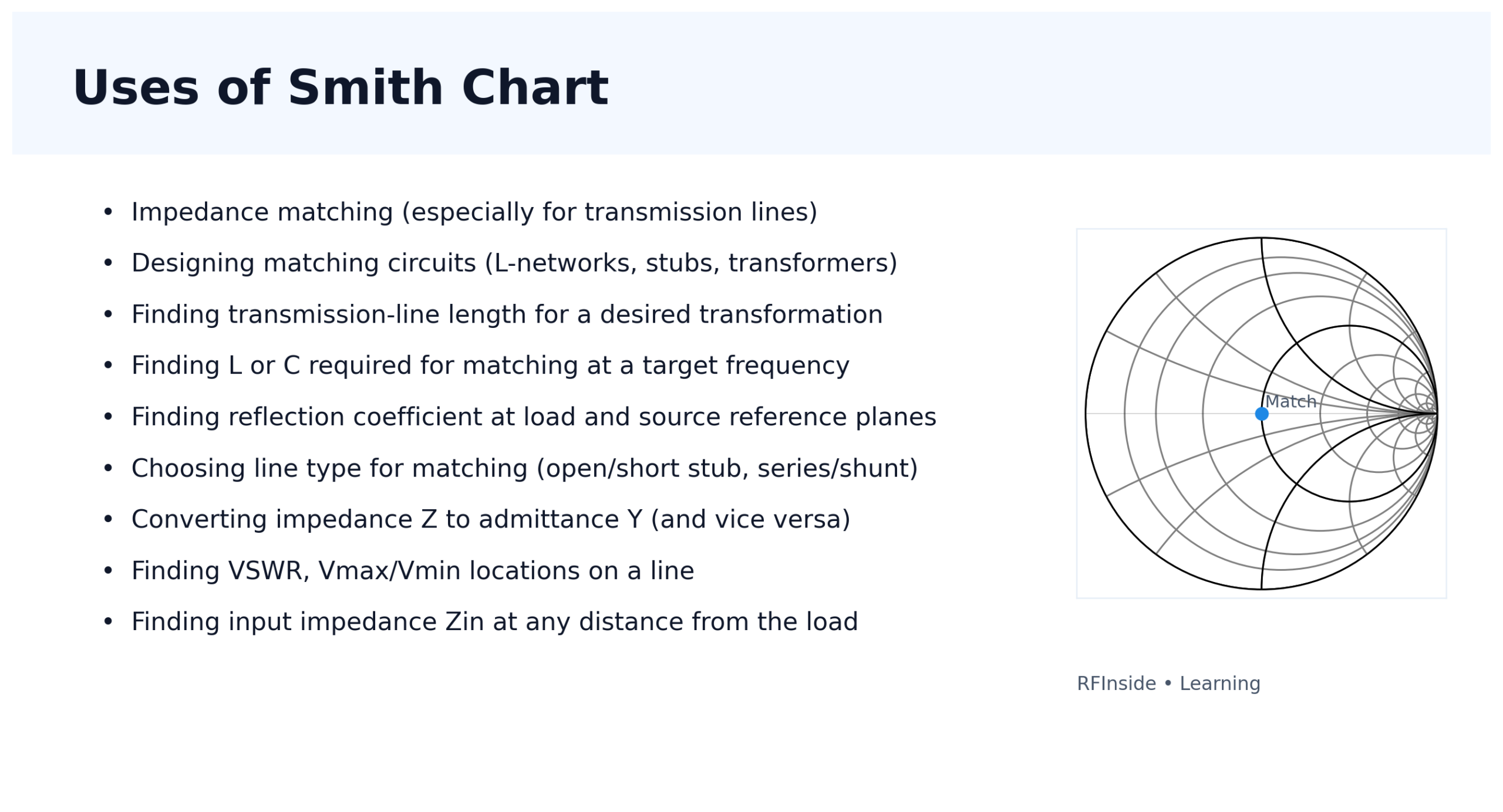
What problems the Smith chart solves
- Impedance matching (especially with transmission lines and stubs)
- Designing matching networks (series/shunt L/C, single-stub, double-stub)
- Finding transmission line length for a desired impedance transformation
- Converting impedance to admittance to handle shunt elements cleanly
- Reading VSWR and return loss directly from |Γ| geometry
- Finding input impedance \(Z_\text{in}\) at any distance from the load
Even if you use VNA/simulator daily, the Smith chart remains one of the fastest ways to “see” whether you need inductive or capacitive correction and whether to do it as a series or shunt element.
Quick reminder
The Smith chart is the unit disk of the reflection coefficient Γ, with impedance/admittance grids overlaid. Center = match, left edge = short, right edge = open.
2) Waves, reflection coefficient Γ, and why impedance “moves”
On a transmission line, voltage and current are superposition of forward and reflected waves: a wave traveling toward the load, and a wave traveling back toward the source. At the load, mismatch creates reflection. The reflection coefficient is defined as the complex ratio of reflected to incident wave amplitude at the load.
Several important things follow immediately:
- If \(Z_L = Z_0\), then Γ = 0 (no reflection, perfect match).
- If \(Z_L \to \infty\) (open), Γ → +1 (full reflection, 0° phase).
- If \(Z_L = 0\) (short), Γ → −1 (full reflection, 180° phase).
- For passive loads, \(|Γ| \le 1\). The Smith chart is literally the unit disk \(|Γ| \le 1\).
Standing waves and VSWR
The interference between forward and reflected waves produces standing-wave patterns. The voltage standing wave ratio (VSWR) is:
Therefore, once you know \(|Γ|\), you know VSWR instantly. On the Smith chart, \(|Γ|\) is simply the distance from the center to the point.
3) Normalization: why we use z = Z/Z0
The Smith chart is drawn for normalized impedance \(z = r + jx\), where: \(r = R/Z_0\) and \(x = X/Z_0\). This makes one chart usable for any characteristic impedance system (50Ω, 75Ω, 100Ω, etc.) — you just normalize before plotting and de-normalize after reading.
Why normalization is non-negotiable
- The chart geometry is derived from Γ, which depends on the ratio \(Z/Z_0\).
- Grid values (r and x) are dimensionless. If you plot raw ohms, the point becomes meaningless.
- Normalization allows quick “scale switching” between different systems.

4) Mapping between normalized impedance z and reflection coefficient Γ
The heart of the Smith chart is the conformal mapping between the impedance plane and the Γ-plane. Starting from the load reflection coefficient:
Divide numerator and denominator by \(Z_0\) and define \(z = Z/Z_0\):
We can also invert this to get z in terms of Γ:
Special points worth memorizing
| Condition | Impedance (z) | Reflection coefficient (Γ) | Where on chart |
|---|---|---|---|
| Perfect match | 1 + j0 | 0 | Center |
| Open circuit | ∞ | +1 | Rightmost edge |
| Short circuit | 0 | −1 | Leftmost edge |
| Purely resistive | r (x=0) | real Γ | Horizontal axis |
| Purely reactive | jx (r=0) | |Γ| = 1 | Outer circle |
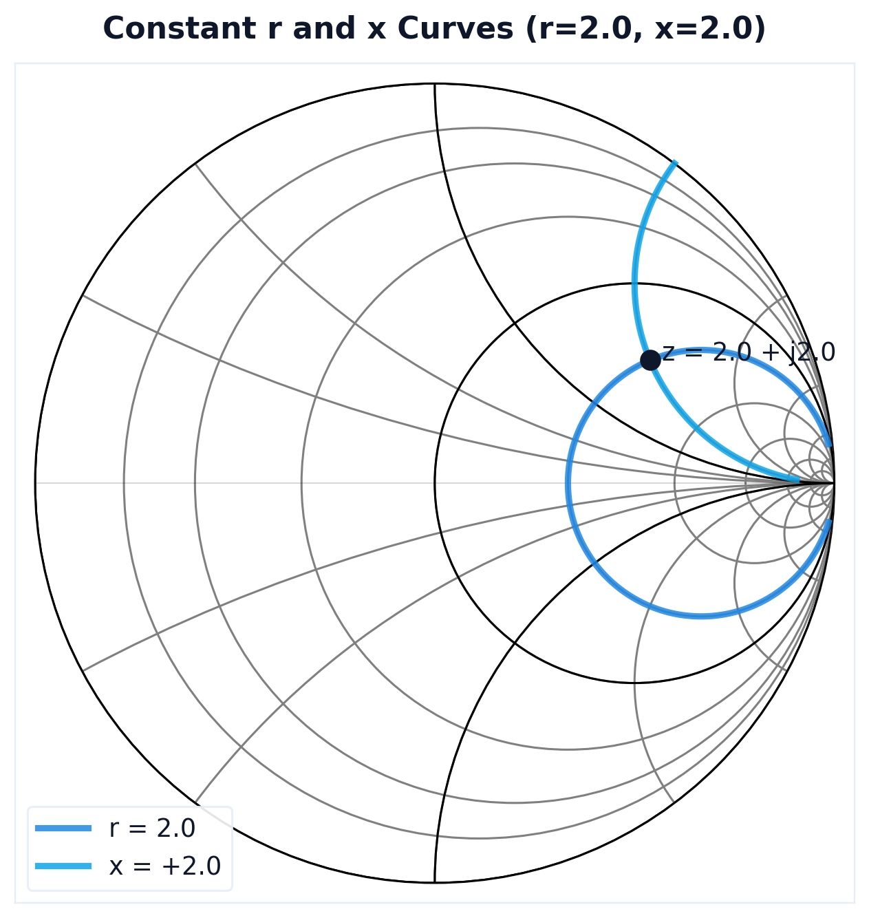
5) Where do the circles/arcs come from? (Derivation)
One reason the Smith chart feels magical is that resistance and reactance become circles. This is not coincidence — it drops out of the Γ mapping. Let Γ = u + jv (Cartesian coordinates in Γ-plane). Let z = r + jx. Using Γ = (z−1)/(z+1), separate real and imaginary parts to show that constant r and constant x form circles.
Result 1: Constant resistance circles
For a fixed r, the locus of Γ is a circle in the Γ-plane with center on the real axis.
Interpretation: for each r, you get a circle centered at \(u = r/(1+r)\) with radius \(1/(1+r)\). When r increases, the circle shrinks and shifts toward the right.
Result 2: Constant reactance arcs
For a fixed x, the locus of Γ is a circle whose center lies on the vertical line u=1.
Interpretation: for each x, you get a circle centered at (1, 1/x) with radius |1/x|. These circles intersect the unit circle and appear as arcs inside the Smith chart.
6) Reading the Smith chart: regions, sign conventions, and fast tricks
6.1 Inductive vs capacitive
The Smith chart’s upper half corresponds to +jX (inductive reactance), and the lower half corresponds to −jX (capacitive reactance). This matches basic circuit theory: \(Z_L = +j\omega L\) and \(Z_C = -j/( \omega C)\).
6.2 The “real axis” is your friend
The horizontal diameter (x=0) contains all purely resistive loads. This line is a powerful reference: most matching networks try to bring your point to the real axis at r=1 (i.e., Z=Z0).
6.3 Three anchor points you should memorize
- Center: z = 1 + j0 (match)
- Left edge: z = 0 (short)
- Right edge: z = ∞ (open)
6.4 What happens when r = 0?
If r=0 (pure reactance), then \(|Γ| = 1\) (100% reflection), meaning your point lies on the unit circle boundary. That’s why the outer circle is the “reactance-only” boundary.
7) VSWR, |Γ|, Return Loss — reading mismatch directly
Once you plot a load on the Smith chart, you automatically know its mismatch severity because mismatch corresponds to the radius \(|Γ|\). The further from the center, the worse the mismatch.
7.1 Return loss and mismatch loss
These are extremely practical in antenna/RF front-end work: return loss tells you what fraction reflects back; mismatch loss tells you how much power you lose purely due to mismatch (even before considering radiation efficiency or conductor/dielectric loss).
7.2 VSWR relationship
8) Moving along a transmission line = rotation on a constant-|Γ| circle
A powerful property of lossless lines: \(|Γ|\) stays constant as you move along the line. Only the phase of Γ changes. Mathematically:
So when you move distance \(l\) toward the generator, Γ rotates by angle \(−2βl\). On the Smith chart, that is a rotation around the center along the same VSWR circle.
Practical rotation rules
- Start at the load point \(z_L\) (or ΓL) on the chart.
- Stay on the same constant-|Γ| circle (VSWR circle).
- Use the outer wavelength scale to rotate “toward generator” by l (in λ).
- After rotation, read the new impedance point \(z_\text{in}\).
9) Impedance ↔ admittance conversion (z ↔ y) and the 180° flip
Matching networks often mix series and shunt elements. Series elements add in impedance, shunt elements add in admittance. That’s why you frequently convert between impedance and admittance views.
The Smith chart offers a beautiful shortcut: to convert a point from impedance to admittance, rotate it by 180° about the center (same |Γ|, opposite angle). This “flip” is exact because: \(y = 1/z\) corresponds to Γ → −Γ.
Algebra check (optional)
If z = r + jx, then:
Note the sign flip on the imaginary component (b = −x/(...)). Graphically, the 180° rotation captures the same behavior.
10) Worked Example A: Plot \(Z_L = 100 + j100\,Ω\) on \(Z_0 = 50\,Ω\)
Let the system characteristic impedance be \(Z_0 = 50\,Ω\). A load is \(Z_L = 100 + j100\,Ω\). First normalize:
Now interpret the location:
- r = 2 means resistance is higher than Z0 → the point sits on the right side of the chart (but not at the edge).
- x = +2 means inductive → point is in the upper half.
- Intersection of the r=2 circle and x=+2 arc gives the location.
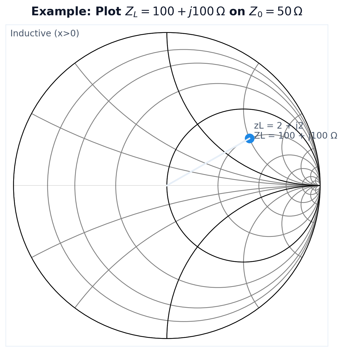
Convert to admittance (common next step for shunt matching)
If you intend to use a shunt stub, convert to admittance:
11) Worked Example B: Input impedance at distance l (Smith chart method + formula)
The input impedance seen at a point distance \(l\) from the load on a lossless line is:
While the formula is exact, it becomes tedious if you do it repeatedly during matching design. The Smith chart does the same transformation visually:
Smith chart procedure (high confidence workflow)
- Normalize: compute \(z_L = Z_L/Z_0\).
- Plot: locate \(z_L\) on the chart.
- Draw VSWR circle: constant-|Γ| circle through \(z_L\).
- Rotate: move along that circle by \(l\) toward generator using the outer “wavelength” scale.
- Read: read \(z_{in}\) (r and x) at the new point.
- De-normalize: \(Z_{in} = Z_0 · z_{in}\).

12) Matching overview: series vs shunt strategy (how engineers decide)
Real-world matching is rarely “one formula”. It is a design choice: series L/C is easy when you can place a component in line; shunt stubs or shunt L/C is easy when you have a good ground and can place a shunt element. The Smith chart helps you pick the most practical topology quickly.
Series matching (impedance view)
- Series elements add reactance: \(Z_{new} = Z_{old} + jX\).
- On chart: you move along a constant resistance circle (r constant), changing x.
- Goal: reach the real axis at r=1 (normalized), or reach a point suitable for a second step.
Shunt matching (admittance view)
- Shunt elements add susceptance: \(Y_{new} = Y_{old} + jB\).
- On chart: flip to admittance and move along constant conductance circles (g constant).
- Goal: reach g=1 (normalized), then cancel b with a shunt element or stub.
13) Single-stub matching (classic Smith chart workflow)
Single-stub matching is one of the most common RF matching methods in microwave PCB work because it uses transmission line sections (low loss at high frequency) instead of lumped parts (which can be lossy or have parasitics at GHz).
13.1 What you are solving
You have a load \(Z_L\) on a line \(Z_0\). You choose a point at distance d from the load, and place a shunt stub there (open or short). The stub provides a susceptance that cancels the residual susceptance, producing a match to \(Z_0\).
Single shunt-stub matching steps (exact Smith chart recipe)
- Normalize and plot \(z_L\) on impedance chart.
- Flip to admittance (rotate 180°) to get \(y_L\).
- Move toward generator along constant-|Γ| circle until you reach a point where g = 1.
- At that point, the admittance is \(y = 1 + jb\).
- Add a stub that provides susceptance \(-jb\) so total becomes 1 + j0.
- Read the distance d from the outer scale and compute stub length from stub susceptance.
13.2 Stub formulas (open vs short)
For a lossless stub with characteristic impedance \(Z_0\) (same line type), its input impedance depends on termination:
In shunt matching you use admittance of stub:
14) Quarter-wave transformer (simple matching for real loads)
If the load is purely real (or close) and narrowband operation is acceptable, the quarter-wave transformer is one of the cleanest matching methods. A λ/4 line transforms impedance according to:
To match \(Z_L\) to \(Z_0\), choose:
When quarter-wave is best
- Load is real (or you can tune it to be near real first).
- You are okay with narrowband matching (frequency sensitive due to λ/4).
- You can realize the transformer impedance in your transmission line technology (microstrip/stripline/CPW).
15) Practical RF layout notes (things textbooks don’t emphasize)
15.1 Real components are not ideal at GHz
Lumped inductors and capacitors have parasitics (ESR, ESL, self-resonance). At high frequency, a “capacitor” may behave inductively above SRF; an inductor may show capacitive behavior. That’s why transmission-line matching (stubs) is often preferred above ~2–3 GHz, depending on component quality.
15.2 Ground quality decides whether shunt matching works
Shunt elements need a low-inductance return. A long via or poor ground can destroy the intended susceptance. If the ground is weak, a series element might be more stable (or use multiple vias / via fence for the shunt).
15.3 Use the Smith chart with measured S11
In antenna tuning, you often start from measured S11 on a VNA. From S11 you already have Γ at the reference plane. If you de-embed to the antenna feed, you can plot it directly. Then you can decide tuning direction (up/down) instantly.
16) Common mistakes + debug checklist (very important)
Mistakes that cause 90% of confusion
- Not normalizing (plotting raw ohms instead of z=Z/Z0).
- Wrong sign convention for reactance (+j is inductive, −j is capacitive).
- Mixing generator/load direction on the wavelength scale.
- Forgetting to flip for admittance when doing shunt stub design.
- Reading the wrong curve (confusing r circles with x arcs).
- Assuming impedance stays constant on line (only |Γ| stays constant for lossless line).
Quick “what component do I need?” cheat sheet
| If your point is… | You likely need… | Why (in one line) |
|---|---|---|
| Above real axis (inductive) | Capacitive correction | To cancel +jX and move downward |
| Below real axis (capacitive) | Inductive correction | To cancel −jX and move upward |
| Right of center (r>1) | Reduce normalized resistance | Use line transform or matching network to reach r=1 |
| Left of center (r<1) | Increase normalized resistance | Transform along line or use L-network |
17) References for further reading
If you want to go beyond intuition and master matching design workflows, these references are excellent:
- David M. Pozar, Microwave Engineering, Wiley — transmission lines, matching, Smith chart usage.
- Robert E. Collin, Foundations for Microwave Engineering — deeper wave/reflection derivations.
- Ramo, Whinnery, Van Duzer, Fields and Waves in Communication Electronics — EM-wave perspective.
- Keysight / Rohde & Schwarz application notes on Smith chart, VSWR, and impedance matching.